

Switched capacitor filter (SCF) or analog Sampled data or commutating filter
Switched capacitor Filters (SCFs) are active IC filters made of op amps, capacitors,
and transistor switches. Also known as analog sampled data Filters or commutating filters, these devices are usually implemented with MOS or CMOS circuits. They can
be designed to operate as high-pass, low-pass, bandpass, or bandstop filters. The primary advantage of SCFs is that they provide a way to make tuned or selective circuits
in an IC without the use of discrete inductors, capacitors, or resistors.
Switched capacitor filters are made of op amps, MOSFET switches, and capacitors.
All components are fully integrated on a single chip, making external discrete components unnecessary. The secret to the SCF is that all resistors are replaced by capacitors
that are switched by MOSFET switches. Resistors are more dificult to make in IC form
and take up far more space on the chip than transistors and capacitors. With switched
capacitors, it is possible to make complex active i lters on a single chip. Other advantages are selectibility of filter type, full adjustability of the cutoff or center frequency,
and full adjustability of bandwidth. One filter circuit can be used for many different
applications and can be set to a wide range of frequencies and bandwidths.
Switched Integrators. The basic building block of SCFs is the classic op amp integrator, as shown in Fig. 1-01(a). The input is applied through a resistor, and the feedback
is provided by a capacitor. With this arrangement, the output is a function of the integral
of the input:

Figure 1-01 IC integrators. (a) Conventional integrator. (b) Switched capacitor integrator
To work over a wide range of frequencies, the integrator RC values must be changed.
Making low and high resistor and capacitor values in IC form is dificult. However, this
problem can be solved by replacing the input resistor with a switched capacitor, as shown
in Fig. 1-01(b). The MOSFET switches are driven by a clock generator whose frequency
is typically 50 to 100 times the maximum frequency of the ac signal to be i ltered. The
resistance of a MOSFET switch when on is usually less than 1000 V. When the switch
is off, its resistance is many megohms.

The clock puts out two phases, designated ϕ1 and ϕ2 , that drive the MOSFET switches. When S1 is on, S2 is off and vice versa. The switches are of the break- beforemake type, which means that one switch opens before the other is closed. When S1 is closed, the charge on the capacitor follows the input signal. Since the clock period and time duration that the switch is on are very short compared to the input signal variation, a brief “sample” of the input voltage remains stored on C1 and S1 turns off.
Now S2
turns on. The charge on capacitor C1
is applied to the summing junction of
the op amp. It discharges, causing a current to Flow in the feedback capacitor C2
. The
resulting output voltage is proportional to the integral of the input. But this time, the
gain of the integrator is

where 𝒇 is the clock frequency. Capacitor C1 , which is switched at a clock frequency of 𝒇 with period T, is equivalent to a resistor value of R 5 T/C1 .
The beauty of this arrangement is that it is not necessary to make resistors on the
IC chip. Instead, capacitors and MOSFET switches, which are smaller than resistors,
are used. Further, since the gain is a function of the ratio of C1
to C2
, the exact capacitor values are less important than their ratio. It is much easier to control the ratio of
matched pairs of capacitors than it is to make precise values of capacitance.
By combining several such switching integrators, it is possible to create low-pass,
high-pass, bandpass, and band-reject Filters of the Butterworth, Chebyshev, elliptical, and
Bessel type with almost any desired selectivity. The center frequency or cutoff frequency
of the Filter is set by the value of the clock frequency. This means that the filter can be
tuned on the l y by varying the clock frequency
A unique but sometimes undesirable characteristic of an SCF is that the output
signal is really a stepped approximation of the input signal. Because of the switching
action of the MOSFETs and the charging and discharging of the capacitors, the signal
takes on a stepped digital form. The higher the clock frequency compared to the frequency of the input signal, the smaller this effect. The signal can be smoothed back into
its original state by passing it through a simple RC low-pass i lter whose cutoff frequency
is set to just above the maximum signal frequency.
Various SCFs are available in IC form, both dedicated single-purpose or universal
versions. Some models can be coni gured as Butterworth, Bessel, Eliptical, or other
formats with as many as eight poles. They can be used for filtering signals up to about
100 kHz. Manufacturers include Linear Technology, Maxim Integrated Products, and
Texas Instruments. One of the most popular is the MF10 made by Texas Instruments. It
is a universal SCF that can be set for low-pass, high-pass, bandpass, or band-reject
operation. It can be used for center or cutoff frequencies up to about 20 kHz. The clock
frequency is about 50 to 100 times the operating frequency.
Commutating Filters. An interesting variation of a switched capacitor filter is the
commutating filter shown in Fig. 1-02. It is made of discrete resistors and capacitors with
MOSFET switches driven by a counter and decoder. The circuit appears to be a low-pass
RC filter, but the switching action makes the circuit function as a bandpass filter. The
operating frequency fout is related to the clock frequency fc
and the number N of switches
and capacitors used.


The bandwidth of the circuit is related to the RC values and number of capacitors
and switches used as follows:

Very high Q and narrow bandwidth can be obtained, and varying the resistor value
makes the bandwidth adjustable
The operating waveforms in Fig. 1-02 show that each capacitor is switched on and
off sequentially so that only one capacitor is connected to the circuit at a time. A sample
of the input voltage is stored as a charge on each capacitor as it is connected to the input.
The capacitor voltage is the average of the voltage variation during the time the switch
connects the capacitor to the circuit.
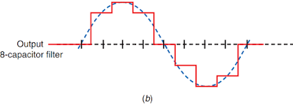
Fig. 1-03(a) shows typical input and output waveforms, assuming a sine wave input.
The output is a stepped approximation of the input because of the sampling action of
the switched capacitors. The steps are large, but their size can be reduced by simply
using a greater number of switches and capacitors. Increasing the number of capacitors
from four to eight, as in Fig. 1-03(b), makes the steps smaller, and thus the output more
closely approximates the input. The steps can be eliminated or greatly minimized by
passing the output through a simple RC low-pass filter whose cutoff is set to the center
frequency value or slightly higher
One characteristic of the commutating filter is that it is sensitive to the harmonics
of the center frequency for which it is designed. Signals whose frequency is some
integer multiple of the center frequency of the filter are also passed by the filter, although
Figure 1-03 Input and output for commutating filter. (a) Four-capacitor filter.
(b) Eight-capacitor filter.


0 Comments
Please give your suggestions in comments.